The Development of Dicing Technology for Silicon Wafer
The growth of the semiconductor industry has always depended on precision manufacturing. One of the most critical steps in chip production is dicing, the process of cutting a silicon wafer into individual dies. From the earliest hand-scribing methods to today’s advanced laser systems, dicing technology has evolved alongside the shrinking dimensions of integrated circuits.
In the early years of wafer production during the 1950s and 1960s, wafers were relatively small, often just one or two inches in diameter. At this scale, manual scribing and breaking was sufficient. Engineers would use diamond-tipped scribers to score the wafer along crystal planes, then carefully snap it apart into rectangular dies. This approach worked for low-volume production but it was slow, inconsistent, and often damaged valuable chips.

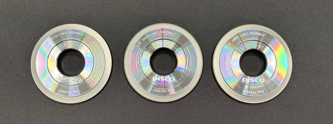
As wafer sizes increased in the 1970s, the industry required a more reliable method. Mechanical sawing with diamond blades became the standard. High-speed rotary saws mounted with fine diamond-embedded blades allowed manufacturers to cut clean, narrow streets between dies. This dramatically improved throughput and reduced die breakage. Companies like DISCO Corporation of Japan established themselves as leaders in this era, producing precision dicing saws that became the backbone of wafer processing worldwide.
The move to larger wafers through the 1980s and 1990s, especially with the transition to 200 millimeter production, pushed dicing technology to adapt again. Blade saws became thinner and more precise, using improved bonding materials and advanced cooling systems to minimize thermal stress. At the same time, manufacturers experimented with scribing and breaking techniques enhanced by automation. Firms such as Accretech (Tokyo Seimitsu) also entered the market, offering automated systems that improved throughput and consistency.
By the 2000s, as feature sizes shrank and wafers reached 300 millimeters, traditional sawing alone was not enough. The industry began adopting laser-based dicing. Laser scribing uses ultraviolet beams to weaken the wafer material along the planned cut lines, followed by mechanical separation. Stealth laser dicing, pioneered and commercialized by DISCO, became a breakthrough. This technique reduces debris, minimizes damage to fragile low-k dielectric layers, and enables narrower streets, allowing more dies per wafer. Other players, including German-based SÜSS MicroTec and U.S. companies like Veeco, explored complementary approaches in photonics and laser applications for semiconductor processing.

Today, the most advanced fabs use a combination of technologies depending on the application. For high-volume, cost-sensitive production, ultra-thin diamond blade saws remain essential. For delicate or high-value chips, especially in advanced nodes or in power devices, stealth laser dicing provides the necessary precision. Plasma dicing, another recent innovation, uses chemical etching to dice wafers without physical contact, reducing mechanical stress on the chips. DISCO again has played a central role in plasma dicing tools, while companies like Panasonic and specialized European firms have explored plasma and laser hybrid approaches.

The development of dicing technology reflects the same pressures that drive the rest of semiconductor manufacturing: the need for higher yield, finer precision, and cost efficiency. From manual scoring to plasma-assisted etching, each advancement has allowed the industry to keep pace with Moore’s Law. The humble act of slicing a wafer has become a highly engineered process, supported by a handful of global equipment manufacturers, and remains critical to delivering billions of chips that power modern electronics.
Silicon Masters incorporates four different dicing blades in it's Evolution Collection Wafer displays.