The History and Production of Ceramic J-Lead Chip Carriers
Ceramic J-lead chip carriers played an important role in the evolution of integrated circuit packaging. Before their introduction, most chips were housed in simple dual in-line packages with leads extending outward. These worked well in the early years of electronics but became a limitation as circuits grew more complex and required denser connections. The J-lead chip carrier offered a more compact, reliable, and thermally stable solution, and it became a standard in many high-performance systems during the 1980s and 1990s.
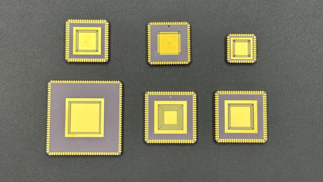
The name “J-lead” comes from the shape of the metal leads that wrap under the sides of the package in a curve resembling the letter J. Instead of extending straight out, the leads bent underneath the ceramic body of the package and made contact with pads on the circuit board. This design allowed for a higher pin count in a smaller footprint, reduced stress on the solder joints, and improved durability in demanding environments. For military, aerospace, and telecommunications equipment, these benefits were significant, and the J-lead package became a trusted format.

The production of ceramic J-lead carriers was a specialized process that required precision and clean manufacturing environments. It began with the creation of the ceramic body, usually made from high-purity alumina. Ceramic was chosen for its strength, stability, and ability to withstand high operating temperatures. Layers of ceramic were pressed and sintered into the required form, with cavities created to house the semiconductor die. Metallized traces were applied onto the ceramic surface to form electrical pathways, often using a combination of molybdenum and manganese that was later plated with nickel and gold for conductivity and bond reliability.
Once the body was complete, the die was attached to the cavity with conductive epoxy or eutectic solder. Wire bonding connected the chip to the package leads through fine gold wires. The J-shaped leads themselves were attached around the perimeter of the carrier, carefully formed and plated to maintain consistency in soldering. The assembly was sealed with a ceramic or metal lid, often using glass frit or solder sealing to ensure hermetic protection against moisture and contaminants.
The leading manufacturers of ceramic J-lead carriers were companies with deep expertise in advanced ceramics and semiconductor packaging. Kyocera in Japan became one of the most important suppliers, leveraging its background in fine ceramics to establish a dominant position in the global market. NTK Technical Ceramics, a division of NGK Spark Plug, also played a major role in supplying high-reliability ceramic carriers. In the United States, companies like CoorsTek, Texas Instruments, and IBM invested in ceramic packaging technologies to support their semiconductor businesses. IBM in particular used ceramic J-lead packages extensively in its mainframes and high-performance computers. European firms such as Siemens and Thomson-CSF also adopted and produced these packages for defense and aerospace applications.
Ceramic J-lead carriers were more expensive than plastic packages, but their performance justified the cost in critical applications. They offered excellent heat dissipation, mechanical strength, and resistance to environmental stress. As surface-mount technology spread, the J-lead design allowed manufacturers to move away from through-hole mounting and achieve higher board densities without sacrificing reliability. This made them ideal for military and space systems, where failure was not an option.
By the late 1990s, however, advances in packaging technology shifted the industry toward plastic quad flat packs and eventually ball grid arrays. These alternatives offered lower costs and even greater pin densities, making them more attractive for consumer electronics and high-volume manufacturing. Ceramic J-lead carriers never disappeared entirely, but their use became concentrated in specialized markets that demanded their reliability and thermal performance.
Today, ceramic J-lead carriers are remembered as a key stepping stone in the evolution of IC packaging. They bridged the gap between the early days of simple packages and the modern era of ultra-dense, fine-pitch interconnects. Their history also illustrates how companies like Kyocera, NTK, and IBM helped shape the semiconductor supply chain by combining ceramic expertise with semiconductor packaging innovation. This period demonstrated that progress in electronics has always depended not only on transistor scaling but also on the parallel evolution of reliable, robust packaging solutions.